- 您现在的位置:买卖IC网 > Sheet目录1991 > CS4340-CZZ (Cirrus Logic Inc)IC DAC 24BIT 96KHZ 101DB 16TSSOP
CS4340
DS297F3
17
The internal serial clock is utilized when additional de-emphasis control is required. Operation in the Internal
Serial Clock mode is identical to operation with an external SCLK synchronized with LRCK; however, External
SCLK mode is recommended for system clocking applications.
4.2.2 External Serial Clock Mode
The device will enter the External Serial Clock Mode whenever 16 low to high transitions are detected on the
SCLK pin during any phase of the LRCK period. The device will revert to Internal Serial Clock Mode if no low
to high transitions are detected on the SCLK pin for 2 consecutive periods of LRCK.
4.3
Digital Interface Format
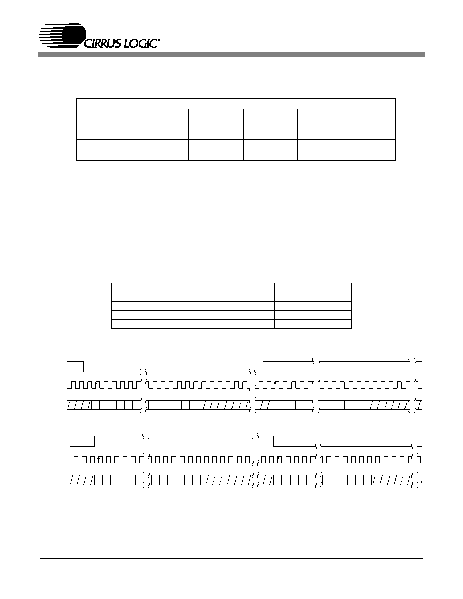
The device will accept audio samples in several digital interface formats as illustrated in Table 5. The desired format
is selected via the DIF1 and DIF0 pins. For an illustration of the required relationship between LRCK, SCLK and
Input
Digital Interface Format Selection
Internal
MCLK/LRCK
Ratio
I2S up to 24
Bits
Left Justified 24
Bits
Right Justified
24 Bits
Right Justified
16 Bits
SCLK/LRCK
Ratio
512, 256, 128
X-
-
X
32
384, 192
XX
X
48
512, 256, 128
-X
X
-
64
Table 4. Internal SCLK/LRCK Ratio
DIF1
DIF0
DESCRIPTION
FORMAT
FIGURE
00
I2S, up to 24-bit data
01
Left Justified, up to 24-bit data
10
Right Justified, 24-bit Data
11
Right Justified, 16-bit Data
Table 5. Digital Interface Format - DIF1 and DIF0
LR C K
SC L K
Left C ha nnel
R ig h t C ha n nel
SDIN
+3 +2 +1
+5 +4
MSB
-1 -2 -3 -4 -5
+3 +2 +1
+5 +4
-1 -2 -3 -4
LSB
MSB
LSB
Figure 15. CS4340 Format 0 - I2S up to 24-Bit Data
LR C K
SC L K
Left C ha nnel
R ig h t C ha n nel
SDIN
+3 +2 +1
+5 +4
MSB
-1 -2 -3 -4 -5
+3 +2 +1
+5 +4
-1 -2 -3 -4
LSB
MSB
LSB
Figure 16. CS4340 Format 1 - Left Justified up to 24-Bit Data
发布紧急采购,3分钟左右您将得到回复。
相关PDF资料
CS4341-CZZ
IC DAC STER 24BIT 96KHZ 16TSSOP
CS4341A-KSZ
IC DAC STER 24BIT 192KHZ 16SOIC
CS4351-DZZ
IC DAC STER 112DB 192KHZ 20TSSOP
CS4352-DZZ
IC DAC STER 102DB 192KHZ 20TSSOP
CS4354-CSZ
IC DAC 24BIT SRL 14SOIC
CS4360-KZZ
IC DAC STER 6CH 102DB 28TSSOP
CS4361-CZZR
IC DAC STER 6CH 105DB 20-TSSOP
CS4362-KQZ
IC DAC 6CH 114DB 192KHZ 48LQFP
相关代理商/技术参数
CS4340-CZZR
功能描述:数模转换器- DAC IC 24Bit 96kHz 101dB Stereo DAC RoHS:否 制造商:Texas Instruments 转换器数量:1 DAC 输出端数量:1 转换速率:2 MSPs 分辨率:16 bit 接口类型:QSPI, SPI, Serial (3-Wire, Microwire) 稳定时间:1 us 最大工作温度:+ 85 C 安装风格:SMD/SMT 封装 / 箱体:SOIC-14 封装:Tube
CS4340-DS
制造商:Cirrus Logic 功能描述:DAC 2CH DELTA-SIGMA 24BIT 16SOIC - Rail/Tube
CS4340-DSZ
功能描述:数模转换器- DAC IC 24Bit 96kHz 101dB Stereo DAC RoHS:否 制造商:Texas Instruments 转换器数量:1 DAC 输出端数量:1 转换速率:2 MSPs 分辨率:16 bit 接口类型:QSPI, SPI, Serial (3-Wire, Microwire) 稳定时间:1 us 最大工作温度:+ 85 C 安装风格:SMD/SMT 封装 / 箱体:SOIC-14 封装:Tube
CS4340-DSZR
功能描述:数模转换器- DAC IC 24Bit 96kHz 101dB Stereo DAC RoHS:否 制造商:Texas Instruments 转换器数量:1 DAC 输出端数量:1 转换速率:2 MSPs 分辨率:16 bit 接口类型:QSPI, SPI, Serial (3-Wire, Microwire) 稳定时间:1 us 最大工作温度:+ 85 C 安装风格:SMD/SMT 封装 / 箱体:SOIC-14 封装:Tube
CS4340-KS
功能描述:数模转换器- DAC IC 24Bit 96kHz 101dB Stereo DAC RoHS:否 制造商:Texas Instruments 转换器数量:1 DAC 输出端数量:1 转换速率:2 MSPs 分辨率:16 bit 接口类型:QSPI, SPI, Serial (3-Wire, Microwire) 稳定时间:1 us 最大工作温度:+ 85 C 安装风格:SMD/SMT 封装 / 箱体:SOIC-14 封装:Tube
CS4340-KSR
功能描述:数模转换器- DAC IC 24Bit 96kHz 101dB Stereo DAC RoHS:否 制造商:Texas Instruments 转换器数量:1 DAC 输出端数量:1 转换速率:2 MSPs 分辨率:16 bit 接口类型:QSPI, SPI, Serial (3-Wire, Microwire) 稳定时间:1 us 最大工作温度:+ 85 C 安装风格:SMD/SMT 封装 / 箱体:SOIC-14 封装:Tube
CS4340-KSZ
功能描述:音频数/模转换器 IC IC 24Bit 96kHz 101dB Stereo DAC RoHS:否 制造商:Texas Instruments 转换器数量: 分辨率:16 bit 接口类型:I2S, UBS 转换速率: 信噪比:98 dB 工作电源电压:5 V DAC 输出端数量:2 工作温度范围:- 25 C to + 85 C 电源电流:23 mA 安装风格:SMD/SMT 封装 / 箱体:TQFP-32 封装:Reel
CS4340-KSZ
制造商:Cirrus Logic 功能描述:D/A Converter (D-A) IC